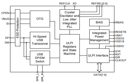
The USB3320C-EZK-TR, developed by Microchip, is a high-performance USB 2.0 ULPI transceiver (PHY) that complies with USB 2.0 OTG as well as host/device standards. It supports High-Speed (480Mbps), Full-Speed (12Mbps), and Low-Speed (1.5Mbps) data transfer modes. Utilizing the ULPI (UTMI+ Low Pin Interface) protocol, it significantly reduces the number of I/O pins required by the host controller, simplifying system design.
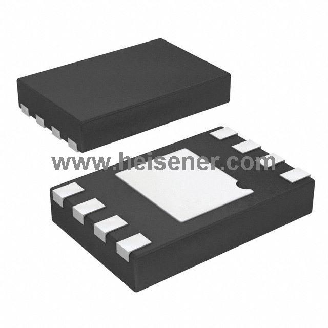
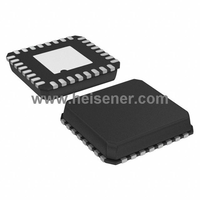
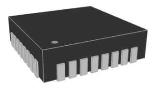
This chip is well-suited for embedded systems, mobile devices, consumer electronics, and industrial control applications. It comes in a compact QFN-32 package and supports 1.8V/3.3V I/O voltages. With built-in voltage regulators, VBUS detection, ID pin identification, and automatic switching features, it ensures reliable performance and low power consumption across a wide range of USB applications.
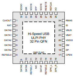
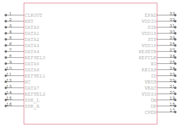
CLKOUT: 60MHz ULPI clock output. Tie to VDDIO to configure as ULPI input clock.
NXT: Indicates when the transceiver is ready for the next byte from the Link.
DATA[0]-[7]: Bi-directional ULPI data bus.
REFSEL[0]-[2]: Selects reference clock frequency.
SPK_L / SPK_R: USB switch I/O for DM / DP signals.
CPEN: Controls external 5V VBUS power switch; low after reset.
DP I/O / DM I/O: USB cable D+ / D− pins.
VDD33: 3.3V regulator output; requires bypass capacitor.
VBAT: Regulator input supply.
VBUS: Connects to external resistor for VBUS detection and pulsing.
ID: USB ID pin; grounded for A-device, floated for B-device.
RBIAS: Connect an 8.06kΩ resistor to GND for internal bias.
XO: External oscillator pin; leave floating when using REFCLK.
REFCLK: 60MHz ULPI input or reference clock output.
RESETB: Active-low reset; tri-states ULPI outputs when low.
VDD18: 1.8V external supply input; requires 0.1µF bypass capacitor.
STP: Stops data transfer from Link to transceiver.
DIR: Indicates bus direction; high when transceiver sends data.
VDDIO: ULPI I/O supply (1.8V–3.3V); determines ULPI signal levels.
GND: Ground.
| Parameter | Specification |
| Manufacturer | Microchip Technology |
| Part Status | Active |
| Protocol | USB 2.0 |
| Number of Drivers/Receivers | 1-Jan |
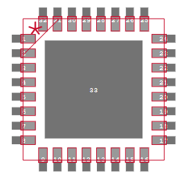
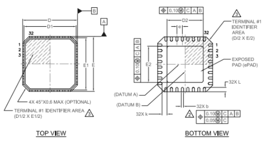
| Package Type | 32-QFN |
| Operating Voltage | 1.8V ~ 3.3V |
| Receiver Hysteresis | 50 mV |
| Operating Temperature | -40°C ~ 85°C |
| Bias Resistor Requirement | External 8.06 kΩ (±1%) |
| RoHS Compliant | Yes |
Integrated ESD protection circuits
Over-Voltage Protection circuit (OVP) protects the VBUS pin from continuous DC voltages up to 30V
Integrated USB Switch
No degradation of Hi-Speed electrical characteristics
Allows single USB port of connection
flexPWR® Technology
UTMI Links with a ULPI bridge
Frequencies: 12, 13, 19.2, 24, 26, 27, 38.4, 52 or 60MHz - pin selectable
External Reference Clock operation available
ULPI Input Clock Mode (60MHz sourced by Link)
Internal Oscillator operation available
Supports Headset Audio Mode
Supports the OTG Host Negotiation Protoco (HNP) and Session Request Protocol (SRP)
UART mode for non-USB serial data transfers
USB3320C-EZK-TR Applications
Networking
Audio Video
Medical
Industrial Computers
Printers
Repeaters
Communication
When using the USB3320C-EZK-TR, it should first be properly soldered onto the PCB, ensuring that all power supply pins (such as VDD18, VDDIO, VBAT, and VDD33) are connected to the appropriate voltage sources and decoupling capacitors are placed to stabilize the power supply. Then, configure the ULPI interface by connecting the data lines (DATA[0:7]), control signals (STP, NXT, DIR), and clock lines (CLKOUT or REFCLK) to establish communication with the main controller. During system initialization, a power-on reset can be performed by pulling the RESETB pin low for at least 1 microsecond and then releasing it.
Depending on the application, function pins such as VBUS, ID, and SPK_L/R can be utilized—for example, the ID pin is used to determine the host/device role in OTG mode. Ensure that an external bias resistor (RBIAS, 8.06kΩ ±1%) is connected to guarantee proper operation of the internal PHY circuitry. Once all configurations are complete, the main controller communicates with the USB3320 via the ULPI protocol, enabling high-speed, full-speed, or low-speed USB data transmission.
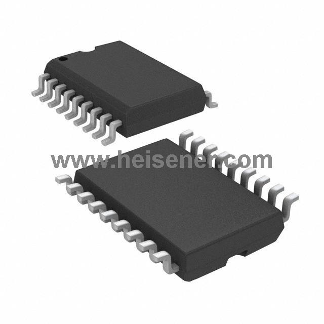
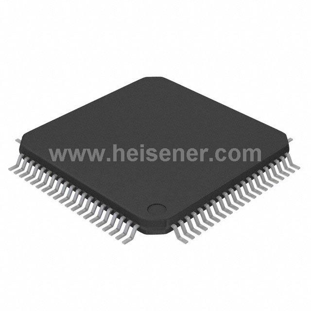
The USB3320C-EZK-TR features a compact 32-QFN package with dimensions of 5mm × 5mm, offering a small footprint and low profile. This package provides excellent thermal and electrical performance, supports surface-mount technology for high-speed automated production, and offers sufficient pins for power, data, control, and functional expansion—making it well-suited for a wide range of USB interface application layouts.
It is a high-speed USB 2.0 ULPI transceiver used for enabling USB host, device, and OTG functions in embedded systems, mobile devices, consumer electronics, and industrial control applications.
Yes, it supports USB OTG with ID pin functionality for role detection and VBUS detection for session management.
It uses the ULPI (UTMI+ Low Pin Interface), which reduces the number of I/O pins needed on the main processor.